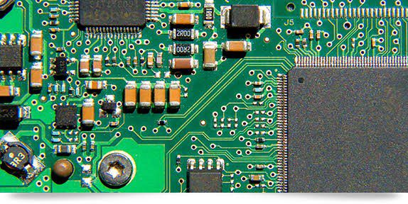
PCB stencils consist of a bare stainless steel sheet, with or without a frame. It has laser-cut openings used for placing solder paste on the printed circuit board. It is done for the surface mount assembly of components. In the PCB stencils, the laser cut on the foil appears on the places where the surface mount devices will go on the PCB board. Solder paste is deposited in these designated places so that components appear in the right places on the board.

To high-precision SMD-Stencils made of stainless steel, you need to determine the nature of your project. Determine what kind of components you need to situate on the circuit board, and accordingly, you can but PCB stencil to transfer solder paste to a bare circuit board. PCB stencil cost depends on the stencil design and configuration. Often the stencils which come with a frame are more costly such as the Framed stencils. You can ask your stencil vendor to align the holes rightly on the stencil board to match the SMD footprint pads on your board layout.
The reflow soldering technology involves the deposition of the solder paste by stencil printing. It is followed by the placement of the components on the solder paste. The final step is the remelting of the solder alloy in the solder paste to solidify the structure. Stencils are the gateway to accurate and repeatable solder paste deposition.
Here are seven things you should know about PCB stencil.
Stencil Thickness
Two major factors determine the stencil thickness and aperture size, i.e., aspect ratio and area ratio. For PCB assembly, the stencil thickness is of paramount importance. The stencil thickness needs to satisfy the QFPs (quad flat package) and BGAs (ball grid array), essentially the surface-mounted integrated circuit packages. You also need to take into account the smallest chip size. For example, a thickness of 0.05mm ? 0.15mm is generally required for solder paste SMT stencil.
Aperture Design
The stencil applied for depositing the solder paste consists of ametal foil, on which apertures are formed that are aligned to the solder pads on the PCB. Aperture size refers to the width and length dimensions of the opening in a PCB stencil. The shape and size of stencil apertures are designed following the corresponding landing pad. It helps to improve the paste deposition and yield.
Printing With Stencil
There are three steps involved in the process of printing with a stencil. The aperture-fill process is the first step in which the apertures are filled with solder paste. The paste transfer process follows it. In this step, the paste in the gap is transferred to the PCB surface. The last step is the positional location of the deposited paste. Together, these three steps are crucial for depositing the solder paste to the correct area on the bare board using a PCB stencil.
Framed Stencil
Framed SMT stencils, also known as “glue-in” stencils, are laser-cut solder paste stencils permanently mounted in a stencil frame. It is the most potent form of laser-cut stencils and consists of a mesh border that helps to stretch the stencil foil within the frame. It is designed for high-volume screen printing. It gives the best locational positional and dimensional accuracy, and it should be operated under controlled temperature conditions. Framed SMT stencil has a 24-hour turnaround standard and is double bonded to prevent extreme wear.
Frameless Stencil
Frameless SMT Stencils are laser-cut solder paste stencils. These are low-cost laser-cut stencils and can work with stencil tensioning systems. Frameless stencil types are not glued to the frame. Therefore, these are less expensive than framed stencils and can deliver high quality and performance at lower costs. Moreover, it has reduced storage space requirements and is suitable for prototyping PCB assembly or short runs.
Prototype SMT Stencils
These stencils are designed for manual solder paste printing applications. Prototype SMT Stencils are custom-made laser cut stencils that are designed for prototyping your PCB board. This stencil eliminates the errors that are prevalent in hand-soldering the prototype PCB.
Electroformed SMT Stencils
These stencils consist of nickel-based, electroforming foils that are designed to function with stencil tensioning systems. The aperture walls are smooth, which provides less surface area for solder paste. As a result, it has the best paste release characteristics. In addition, the nickel configuration of the stencil offers a lower friction coefficient in comparison to stainless steel.
Stencil Alignment
For perfecting the marking of the solder paste on the PCB pads, ‘fiducial marks’ (registration marks) are added to both PCB and stencil. With these marks, it helps to achieve a perfect alignment between the PCB and the stencil.
To Conclude:
These are some of the technical aspects that are a part of the stencil printing process. PCB stencil, in contrast to the hand soldering process, offers consistency and saves time. It provides a fast, mass solder paste deposition process and is suitable for mass production.

As the editor of the blog, She curate insightful content that sparks curiosity and fosters learning. With a passion for storytelling and a keen eye for detail, she strive to bring diverse perspectives and engaging narratives to readers, ensuring every piece informs, inspires, and enriches.


